Table of Contents
SLICE-FPGA-II Manual
Model No. SLICE-FPGA-II
Document Last Updated on 2023/08/08 23:20
Please read Limited Warranty and General Warnings and Cautions prior to operating the SLICE-FPGA-II.
Links
Click here for the Main Manuals Page.
Click here for the FFC-100 Quick Start Guide.
Click here for the FFC-100 API.
Description
The SLICE-FPGA-II is an FPGA-based locking instrument for use with a Fiber Frequency Comb such as the FFC-100. The included software allows for seamless locking of both the Carrier Envelope Offset and Optical frequencies.
Contents
The contents of the SLICE-FPGA-II box includes
- SLICE-FPGA-II
- USB memory stick with WinPython-64bit-3.6.1.0Qt5 and control software
- Power cord for your ship-to country
- An Ethernet cable for connecting your SLICE-FPGA-II to a computer.
Ensure that you received all of the materials. If you did not receive all of the materials, contact us at [email protected]
List of Warning Symbols
 | Warning. Pay special attention to procedures and notes. If procedure is not followed carefully, damage to the SLICE-FPGA-II or devices connected to it may occur. |
 | Potential for electrical shock hazard. |
Absolute Maximum Ratings and Power Input
Note: All modules designed to be operated in a laboratory environment.
Notice
| | Do not block the airflow vents on the side of the chassis or the fan inputs & outputs on either the FFC-100 or the SLICE-FPGA-II. |
| If this instrument is used in a manner not specified by the manufacturer in this manual or other relevant literature, protection provided by the instrument may be impaired. | |
| Successful implementation of the SLICE-FPGA-II depends critically on the design of the whole system: Frequency Comb, phase locking electronics, and any references to which the Frequency Comb is locked or vice versa. |
Specifications
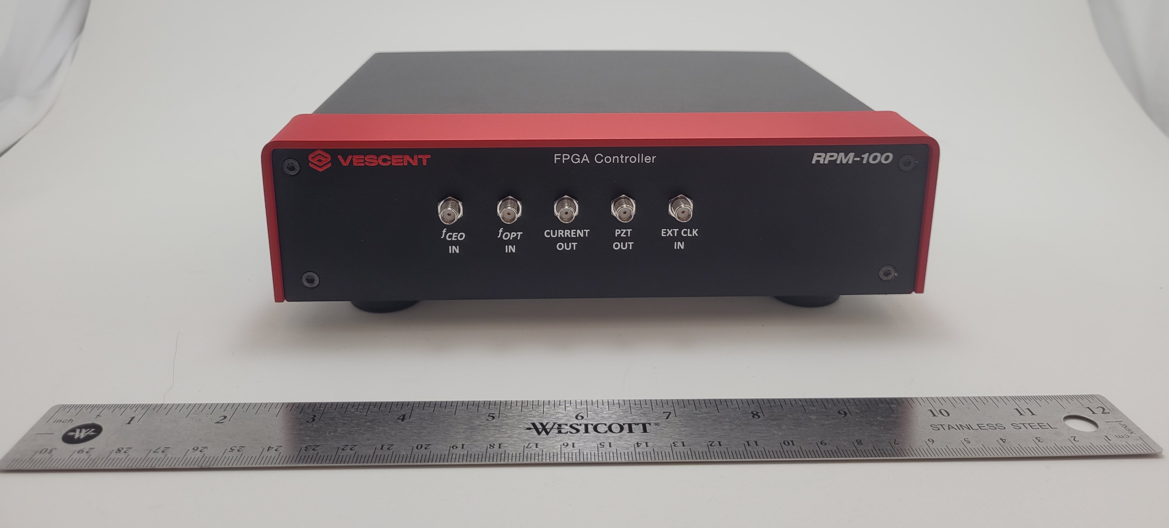
Front Panel
 Fig. 2: Front Panel of the SLICE-FPGA-II
- fCEO input (SMA)
- fOPT input (SMA)
- Current output for modulating pump diode
- PZT modulation output to modulate PZT
- External Clock Input. Use requires specifying input frequency in the settings menu.
Back Panel
 Fig. 3: Back Panel of the SLICE-FPGA-II
- AC power entry module and fuse
- Extension port (unused)
- Reference Clock signal (+3V 10MHz) for clocking external equipment
- Analog Slow Servo control voltage (±10V)
- Ethernet port for communication with a computer
Software Setup
- Install WinPython (WinPython-64bit-3.6.1.0Qt5) from the USB memory stick provided with the SLICE-FPGA-II in an easy to remember location. Do not use “WinPython-64bit-3.6.1.0Qt5” from the sourceforge.net or Github.net websites.
- Open the WinPython folder after installing WinPython, and launch the WinPython terminal within this folder.
- Navigate to the “digital_servo_python_SLICE-FPGA-II” folder and type “python XEM_GUI3.py” to start the GUI.

- A start-up menu should appear (figure 5). Check that the software can recognize the ethernet connection to the module. If the module is recognized, the device name and IP address will appear next to “Connected FPGAs”. If the device is not initially found, click “Broadcast discovery packet” to search for the device.
- If your computer does not see the SLICE-FPGA-II in the start up screen, consult the troubleshooting guide for additional help.

- If you received your SLICE FPGA prior to 7/20/23, ensure “Push default values to Red Pitaya” is selected and press OK.
- If you received your SLICE FPGA after 7/20/23, ensure the center option is selected, labeled “Connect to a Red Pitaya with its current settings”. If the default values of your SLICE FPGA II have been overwritten, the original values can be recovered by importing the XML file titled with your devices serial number. To do this, once connected to the FPGA, open the settings tab. In the Settings Management window enter the proper filename corresponding to your FFC serial number, and click “Import All Settings from File” (figure 5).

FPGA Control
The SLICE-FPGA-II FPGA Controller can be used to phase lock ƒCEO to a reference and ƒOPT to a reference laser such as the Rio Planex. The SLICE-FPGA-II should be connected to a Vescent frequency comb (FFC or Comb Module) as shown below (figure 7).
 Fig. 7: System Level Diagram of the SLICE-FPGA-II Connected to an FFC-100
Locking fopt requires a reference CW laser and heterodyne setup (such as a 50:50 beam splitter and DWDM filter). The stability of the lock will depend on the reference laser used. All Vescent performance data is collected with a Rio Planex laser.
External Clock
The external clock input (#5 on the Front Panel Diagram) allows the FPGA to be clocked with an external source, e.g. fREP from the FFC, or another system’s master clock. Navigate to the “Settings” tab and select the appropriate clock signal to be used (figure 8). Enter the incoming clock’s frequency (in Hz) into the “Target ExtClk Freq” box, press enter, and then press the “External clock” button above

The SLICE-FPGA-II accepts a variety of discrete clock signal frequencies (15, 20, 25, 30, 40, 50, 75, 100, 125, 150, 200 and 250 MHz). Due to limitations of the internal dividers of the FPGA, certain external clock frequencies will result in an inaccurate absolute frequency reference. If a clock frequency other than those provided is required, please contact Vescent staff to discuss your application.
Locking ƒ(CEO)
- Navigate to the “CEO Lock” tab and enable the “Auto-refresh” button in the top left of the window. Set your desired RF lock frequency of the Fceo beatnote in the “Reference Frequency [Hz]” input. Adjust the “Offset DAC 0” slider near the top left by clicking and dragging the slider until the Beatnote is roughly centered in the red filter trace (figure 9). It is also possible to adjust the FFC-100 oscillator current on its front panel to make this adjustment.
- Press the “Lock” button (figure 10, top middle). If the system doesn’t lock, change the VCO sign to the opposite polarity (top right) and try again. A warning may occur if the selected VCO sign is incorrect. If the system still won't lock, try lowering the Kp value (bottom left).
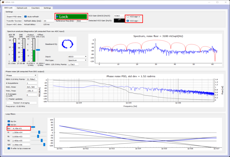 Fig. 10: Locking ƒ(CEO)
 - If the Beatnote is properly locked, the integrated phase noise value listed in the center of the window should be close to the value listed in your devices CoC.


Locking ƒ(opt)
- Ensure that your laser reference source is properly mixed with the “EDFA Out” optical port of the frequency comb as described in the devices CoC and is input back into the device via the “ƒopt” input port at a power level of <1.5 mW.
- Navigate to the “Optical Lock” window and enable the “Auto-refresh” button in the top left of the window. Set your desired RF lock frequency of the ƒopt beatnote in the “Reference Frequency [Hz]” input. Adjust the “Offset DAC 1” slider near the top left by clicking and dragging the slider until the Beatnote is roughly centered in the red filter trace (figure 11).
- Press the “Lock” button (figure 12, top middle). If the system doesn’t lock, change the VCO sign to the opposite polarity (top right) and try again. A warning may occur if the selected VCO sign is incorrect. If the system still won't lock, try lowering the Kp value (bottom center).
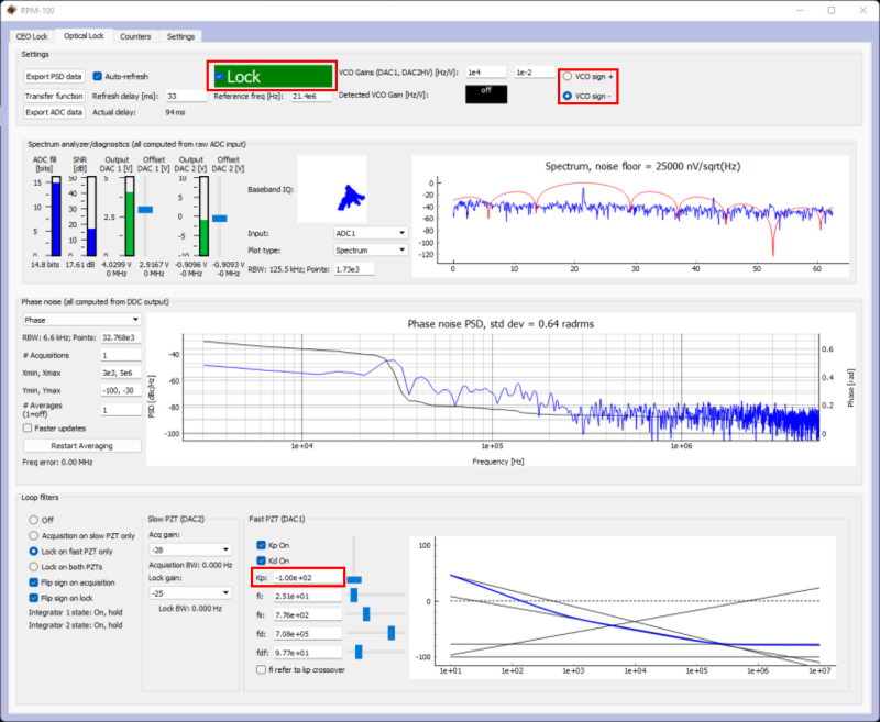 Fig. 12: Locking ƒ(opt)
- If the Beatnote is properly locked, the integrated phase noise value listed in the center of the window should be close to the value listed in your devices CoC.
- Adjust PID settings (bottom of figure 10 and figure 12) as needed to lower the integrated phase noise of each parameter (fCEO and fopt). The default settings provided in the software are tuned for your specific device but tweaking the values can often improve performance based on the noise characteristics of your environment.


Troubleshooting
Overview
In many cases, all that is necessary to get up-and-running with the SLICE-FPGA-II is to install the correct WinPython distribution, and run the provided GUI software using the WinPython terminal. If you are unable to connect the GUI to the SLICE-FPGA-II, follow the below instructions to eliminate possible causes of failure.
Ethernet Controller IP Configuration
Whatever ethernet port you use to control the SLICE-FPGA-II, it is necessary that your computer identifies itself on this Ethernet port with a fixed IP address in the 192.168.0.x subnet. Sometimes a computer’s default settings do not fit this requirement. From the Windows Control Panel, click through: Network and Internet –> Network and Sharing Center –> Change adapter settings
You will see a number of network adapters listed. You should see one of the network adapters change state when you connect the powered-on SLICE-FPGA-II to your PC via the ethernet cable, as shown below:

Watch for this change to identify the correct network adapter.
- Right-click on the adapter, and click Properties.
- From the screen that appears, click on “Internet Protocol Version 4 (TCP/IPv4)” and then click Properties.
 Fig. 13: The Adapter Properties screen, with the IPv4 Settings highlighted
- In the IPv4 Properties Page, select the bubble next to “Use the following IP address:”, and fill in the IP Address to be 192.168.0.xxx, where xxx is an integer from 0 to 255, and not 150, as that is the address used by the SLICE-FPGA-II. In this example, we used 196.
 Fig. 14: The IPv4 Properties page, with the IP Address and Subnet Mask filled in.
The Subnet Mask will default to 255.255.255.0, which is fine.
NOTE: If you use this same Ethernet port to connect to another network, these configuration changes could result in connectivity problems with that network. If this poses a problem for you, consider buying a USB-to-Ethernet adapter, and configuring just that adapter for use with the SLICE-FPGA-II.
Windows Firewall Rules
If you continue to have trouble connecting to the SLICE-FPGA-II, it’s possible that your firewall settings are blocking communications with the device. From the Windows Control Panel, click on System and Security –> Windows Defender Firewall –> Advanced Settings to open up the Windows Defender Firewall with Advanced Security manager application. In the left panel of the program, click “Inbound Rules.” Then, in the right-hand panel of the program, click “New Rule…” Use the “New Inbound Rule Wizard” to create a new rule to the following specifications:
- Rule Type: Program
- Program: [WINPYTHON INSTALL DIRECTORY]\WinPython-64bit-3.6.1.0Qt5\python-3.6.1.amd64\python.exe
- Action: Allow the connection
- Profile: Domain, Private, and Public
- Name: Red Pitaya WinPython (or another name of your choice)
In the left-hand panel, click “Outbound Rules”, and then click “New Rule…”. Repeat the above Rule creation steps to create a rule that allows outgoing packets from the WinPython directory’s “python.exe” file. Finally, ensure that the aforementioned python.exe file is not being restricted by any other firewall rules.